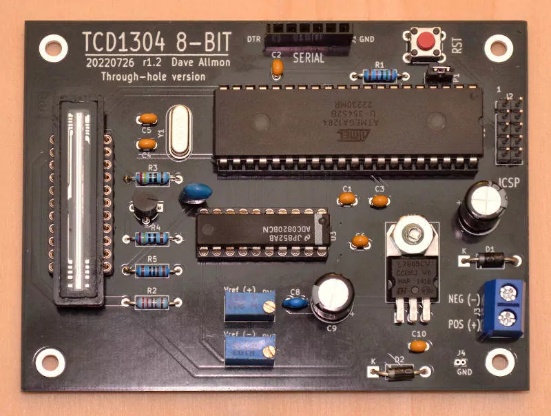
8-bit TCD1304 Spectrograph Board
An Arduino can't really keep up with a CCD using the internal analog to digital converter, but with an external 8-bit half-flash ADC it's no problem at all. The ADC is the TI ADC0820, which can digitize up to 666k samples per second. The sample rate here works out to be a hair over 222kSPS using the code below. The 3694 pixel frame takes around 16.66mS to read and digitize, and around 4 seconds to download at 115.2k baud.
Hardware
Microcontroller
The Arduino Uno doesn't have enough RAM for a 3694 pixel buffer. That leaves either the Arduino Mega2560 with 4kB or a standalone ATmega1284 with 16kB RAM. It wouldn't be easy to embed an Arduino Mega2560, so I went with the ATmega1284. You don't need the "P" part. There is no power control in this project.
Analog to Digital Converter
The project uses the ADC0820CCN, which is in a DIP package. The ADC0820 ADC has + and - reference inputs designed to set the range of the ADC, so you can focus on the interesting portion of the input range, keeping full 8-bit resolution. The ADC0820BCN part has ±1/2 LSB linearity. The ADC0820CCN has ±1 LSB linearity. Either is fine for this project. The ADC0820BCN costs considerably more than the ADC0820CCN.
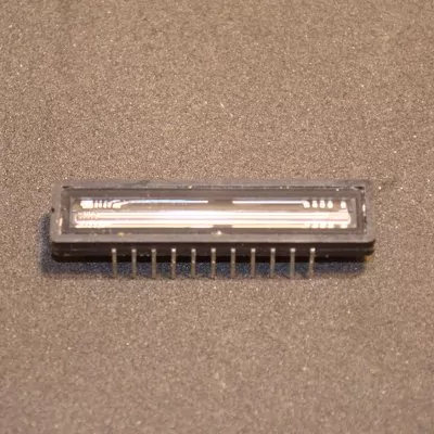
Linear Array CCD
The CCD is a Toshiba TCD1304AP 3648 pixel linear CCD sensor which requires only a single supply voltage. The sensor is driven
directly by the microcontroller, and the analog output is buffered by a transistor. The
MCLK signal is 888.88kHz, and the pixels are read at 222,220 pixels per second. That's a limitation of the
microcontroller and ADC - not the CCD.
The TCD1304AP CCD is available on ebay or aliexpress for anywhere from $8 to $40. Mouser has new ones (TCD1304DG) for $36.
KiCAD Project Files
Assuming you have KiCAD installed, go to the folder you want to be the parent of the project, like "/home/<your_username>/dev", and unzip the zip file. It will create a directory "8-bit-spect-th" contaiing all the project's files. Double-click on the "8-bit-spect-1284.pro" file and KiCAD will load it.
nSchematic Diagram

Description
A timer on the ATmega1284 generates an 888.88kHz squarewave to be used as the MCLK signal. The code that
toggles the clocks on the CCD and ADC does so in cadence with the MCLK signal. The clock edges are aligned
by an adjustment of the timer one cycle before the line is read. MCLK runs continuously. The SH,
ICG, WR, and RD are only asserted when the CCD is being read.
The output of the CCD is buffered by a PNP transistor before being sent to the ADC. The previous version used an OpAmp to invert and amplify the CCD output to the full range of the ADC. This proved to be unnecessary and added another adjustment. The ADC range is configurable, and it's a simple matter to subtract the pixel value from 255 to invert it.
The original firmware read the CCD continuously and just dumped the buffer when you asked for it. This version does not do that. It reads the buffer on demand. That freed up the main loop to do other things. The firmware reads the CCD 4 times to clear it before exposing, and 99% of the time that is enough. If it has been sitting idle for more than a few minutes with light hitting it, the electrons will flood over the surface and reading it four times will not be enough. If you take a reading and see nothing but a vertical line on the readout, that is probably what happened. Just read it again to clear it. If it still doesn't clear, try reducing the exposure time.
ICSP Connector and JP1
At the pin 1 end of the microcontroller is a programming connector. Beside pin 3 is a jumper marked JP1. The
programming connector is for burning the bootloader into the ATmega1284. Jumper JP1, when installed, passes
programmer power to the circuit to allow programming with no other power source. When the JP1 is removed,
the programmer is isolated. That is how it should normally be to keep from having collisions between the on-board 5V and
the programmer's 5V.
Serial Connector
There is a serial connector that matches the FTDI pinout. It's used for uploading the firmware and for sending commands and downloading the
video data. The board is marked with DTR on one end of the connector and GND on the other. If you hook it up
backwards it shouldn't do too much damage. The pins that would be dangerous are not connected. Make the connector female if you have
a male connector on your USB to TTL converter.
RV1 and RV2
Trimmer pots RV1 and RV2 are for adjusting the black level and white level respectively. Don't use cheap pots.
Use Bourns if you can get them. The cheap ones act really flakey at the ends of their ranges, and will give you fits trying to fine tune
the calibration.
Other Parts
Diode D1 is there to protect the circuit should someone accidentally hook the power up backwards. Diode D2 is there
for when you disconnect the power. It keeps the regulator from becoming reverse biased. The switch marked RST is the reset on the
ATmega1284. Just in case you are working on code, and it hangs on you. It's better than disconnecting the power and reconnecting.
I have a few blank PC boards available again that I can ship to US addresses. $10.00 delivered via USPS. They use the DIP packaged ADC0820, instead of the SOIC version. Ping me on the Contact Form if you are interested.
Assembly
Assembly is straightforward, but be aware that the CCD requires a 22 pin socket with a width of 400 mils (10.16mm). You can use female machined pin headers, which I have done in a pinch, but this time I did use a socket.
If you are wiring it up on a proto board, Be careful to keep the digital clocks and analog wiring away from each other where possible. Use 0.1µF bypass capacitors at every Vcc connection. Keep all the digital wires as short as practical to keep them from radiating more than necessary. Be especially careful when routing the MCLK signal near analog areas. That is the only external signal that is toggling while the ADC is integrating the analog signal.
I had a little noise that you can see in the Calibration section below. The circuit is sensitive to high frequency power supply noise. That means the little switching power supplies are pretty much out. You'll want to use a linear power supply rather than a switcher. They are available from Jameco. 12V will work, but 9V @ 600mA is perfect. If you use a 12V supply, make sure it's regulated. The 9V supply doesn't need to be. You can tell the linear supplies because they have inputs of 120V 60Hz, rather than 100-240V 50-60Hz. Jameco actually says linear in the description of their linear supplies, but then other places say linear even on their switchers. I guess what I'm trying to say is don't look for a linear wall-wart on ebay. When I switched to a linear supply, the noise almost completely disappeared and I get essentially flat lines for minimum exposures.
Software
Use the MightyCore boards manager plugin by MCUdude. The board will be ATmega1284 and the variant will be the 1284 or the 1284P, depending on which one you have. Pinout is "standard" and the frequency is 16MHz. You can add the MightyCore boards to the boards manager by adding the following url to the "Additional Boards Manager URLs" textbox in Arduino preferences:
https://mcudude.github.io/MightyCore/package_MCUdude_MightyCore_index.json
Then just open the Boards Manager under Tools->Board->Boards Manager and go to the bottom to install the MightyCore boards. The selection of boards will increase considerably to include all the ATmegaxx4 chips, ATmega16/32, and ATmega8535. The bootloader should be the MightyCore 1284. Additional programmers will appear, too, and you should use one of them with the MightyCore bootloader.
You will need an AVR programmer to burn the Arduino bootloader into the ATmega1284. The board uses a 10-pin ICSP connector. The USB-serial converter you use will need to have its LED removed or disabled, or just covered well.
The source code for the linear CCD application is very carefully crafted in places to maintain the phase relationship between all the CCD clocks and stay true to the specification. It takes a logic analyzer to validate the results of any code changes in the "readLine()" function. There is a looping function in the code. That is for diagnostics - so you can check the timing, if you are developing the code.
#include <util/delay_basic.h>

// ADC RD signal pin 17
#define RD 0x08

// ADC write signal pin 18
#define WR 0x10

// CCD Shift Gate pin 19
#define SH 0x20

// CCD Integration Clear Gate pin 20
#define ICG 0x40

// CCD Master clock pin 21
#define MCLK 0x80

// CCD and ADC clocks
#define CLOCKS PORTD
#define CLOCKP PIND

// ADC data
#define ADATA PINC

#define PIXEL_COUNT 3694

uint8_t pixBuf[PIXEL_COUNT];
char cmdBuffer[16];
int cmdIndex;
int cmdRecvd = 0;
int exposureTime = 10;
bool looping = false;

void setup() {
  // Initialize the clocks.
  DDRD |= (WR | SH | ICG | MCLK | RD);  // Set the clock lines to outputs
  CLOCKS = (ICG + RD + WR);       // Set the ICG, RD, and WR high.

  // Setup the ADC data port as inputs.
//  DDRC = 0;

  // Enable the serial port.
  Serial.begin(115200);

  // Setup timer2 to generate an 888.8kHz frequency on pin 21
  TCCR2A = (0 << COM2A1) | (1 << COM2A0) | (1 << WGM21) | (0 << WGM20);
  TCCR2B = (0 << WGM22) | (1 << CS20);
  OCR2A = 8;
  TCNT2 = 1;
}

void readLine() {

  // Get a pointer to the buffer.
  uint8_t *buf = pixBuf;
  int x = 0;
  uint8_t scratch = 0;

  // Disable interrupts or the timer will get us.
  cli();

  // Synchronize with MCLK and
  // set ICG low and SH high.
  scratch = CLOCKS;
  scratch &= ~ICG;
  scratch |= SH;
  while(!(CLOCKP & MCLK));
  while((CLOCKP & MCLK));
  TCNT2 = 0;
  _delay_loop_1(1);
  __asm__("nop");
  __asm__("nop");
  __asm__("nop");
  __asm__("nop");
  __asm__("nop");
  CLOCKS = scratch;

  // Wait the remainder of 4.5uS @ 16MHz.
  _delay_loop_1(22);
  __asm__("nop");
  __asm__("nop");

  // Set SH low.
  CLOCKS ^= SH;

  // Wait the remainder of 4.5uS.
  _delay_loop_1(23);

  // Start the readout loop at the first pixel.
  CLOCKS |= (RD + WR + ICG + SH);

  do {
    // Wait a minimum of 250nS for acquisition.
    _delay_loop_1(2);

    // Start the conversion.
    CLOCKS &= ~WR;
    _delay_loop_1(3);
    CLOCKS |= WR;

    // Wait the rest of 2uS for conversion.
    _delay_loop_1(9);

    // Read the result.
    CLOCKS &= ~RD;

    _delay_loop_1(3);
    __asm__("nop");
    __asm__("nop");
    *buf++ = ADATA;

    // Set the clocks back to idle state
    CLOCKS |= RD;

    // Toggle SH for the next pixel.
    CLOCKS ^= SH;

  } while (++x < PIXEL_COUNT);
  CLOCKS = (ICG + RD + WR);
  sei();
}

void sendData(void) {

  int x;

  for (x = 30; x < 3678; ++x) {

    Serial.print(x - 30);
    Serial.print(",");
    Serial.print(255-pixBuf[x]);
    Serial.print("\n");
  }
}


void loop() {

  int x;
  char ch;

  if (cmdRecvd) {
    if (cmdBuffer[0] == 'r') {

      // Clear any residual charge.
      for (x = 0; x < 6; ++x) {
        readLine();
      }

      // Expose.
      delay(exposureTime);

      // Read and send data.
      readLine();
      sendData();

    } else if (cmdBuffer[0] == 'e') {
      String tmp = String(&cmdBuffer[1]);
      exposureTime = tmp.toInt();
      if (!exposureTime) {
        exposureTime = 1;
      }

    } else if (cmdBuffer[0] == 'l') {
      looping = !looping;
    }
    memset(cmdBuffer, 0, sizeof(cmdBuffer));
    cmdRecvd = 0;
    cmdIndex = 0;
  }
  if (looping) {
      readLine();
      readLine();
      delay(exposureTime);
      readLine();
  }
  while (Serial.available() > 0) {

    ch = Serial.read();

    if (ch != 0x0a) {
      cmdBuffer[cmdIndex++] = ch;
    } else {
      cmdRecvd = 1;
    }
  }
}
Timing
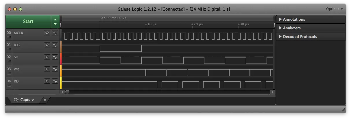
At time 0s:0ms:0µs you can see the MCLK is stretched a little. That is to get the ICG, SH, WR and RD lines in sync with the timer, which generates the 888kHz MCLK signal. The code has to maintain this timing relationship throughout the entire read process, reading one pixel every four MCLK cycles. The readLine() function is riddled with assembly language "NOP" code to keep the timing precise. Keep in mind that adding even a single machine instruction requires re-factoring the read timing.
The Sampler Program
The Sampler program is written for Python 3. You must also install pyserial pip install pyserial. You must also install tkinter. Do a search on how
to install tkinter on your operating system. The first couple of results are good.
A few lines up from the end of the python code is a line:
app = Application(master=root, port="/dev/ttyUSB0", exposure=50)
It should match your serial port. If you are using Windows, change that to something like:
app = Application(master=root, port="COM3", exposure=50)
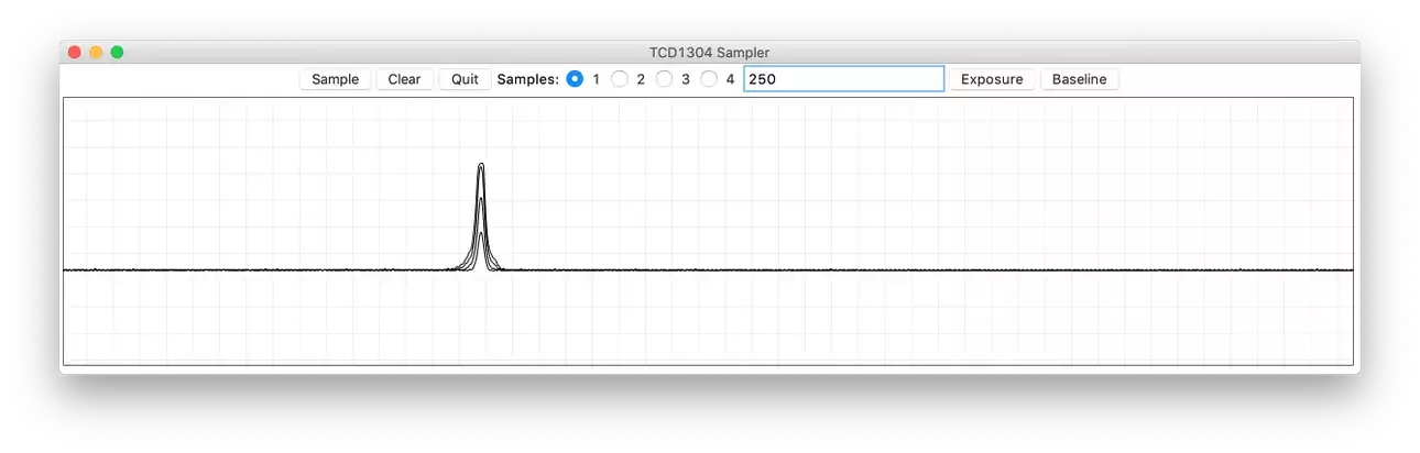
Again, make it match the serial port you are using. If the app ends with return code 1, it didn't find the port. When you click Sample, it draws a graph of the CCD output, but also makes a file in the program directory named 'ccd.csv'. That file can be imported into a spreadsheet application for further processing, including making a graph at the full resolution of the CCD.
The horizontal resolution of the sensor, and the data returned, is three times the resolution of the graph. The csv file is written at full resolution. The pixels are binned into 3-pixel wide buckets for the graph.
The buttons are:
- Sample - Read the CCD and put the trace on the screen.
- Clear - Clear all traces from the screen.
- Quit - End the program.
- Samples - How many scans to average together (removes a little noise, but slow).
- Exposure - An integer value from 1 to 1000. The milliseconds to expose.
When you click on Sample, it draws the graph. It does not erase the previous line. The Clear button does that. If you have an exceptional build and don't have any annoying noise, the Samples radio buttons won't help at all.
If you ever get what looks like a saturated signal, first just redo the exposure. CCDs gather light whether you read them or not, so leaving it alone for 30 minutes is like taking a 30-minute exposure. The code reads the frame 4 times before exposing, but sometimes that isn't enough to get all the electrons out of the system.
Calibration
To calibrate, start by setting the RV1 pot, "Vref (+)", all of the way clockwise. Set RV2, "Vref (-)" all of the
way counter-clockwise. This sets the black level at 5V and the white level at 0V.
Get a piece of black electrical tape long enough to cover the ccd + 1/4 inch on each end. Cut a slit across the tape, but not
all the way - just in the center. Use an X-acto knife or similar. Then cover the CCD with the electrical tape in a room
with dimmed lighting. The tape will come off without damaging the CCD. You should see a spike when you make a sample. If not,
increase the exposure time. If the spike looks more like a square pulse, decrease the exposure time. If you rub your finger
down the length of the tape on the CCD, starting at the slit, it will open the slit wider, if you need it. Rubbing your finger
toward the slit will tend to close it.
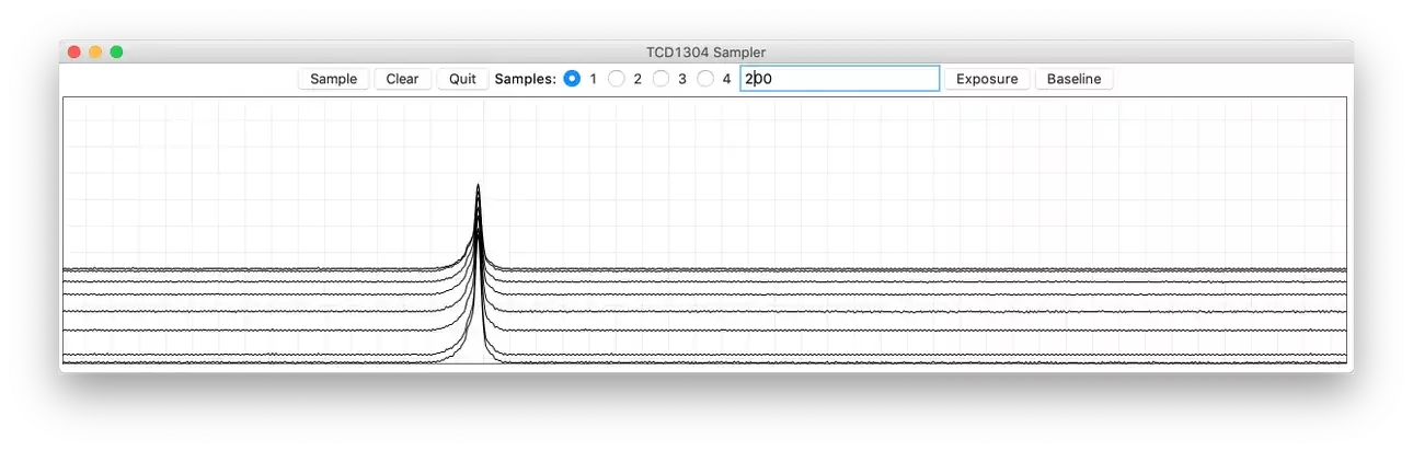
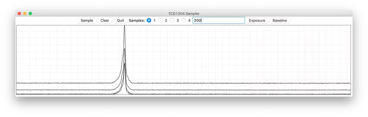
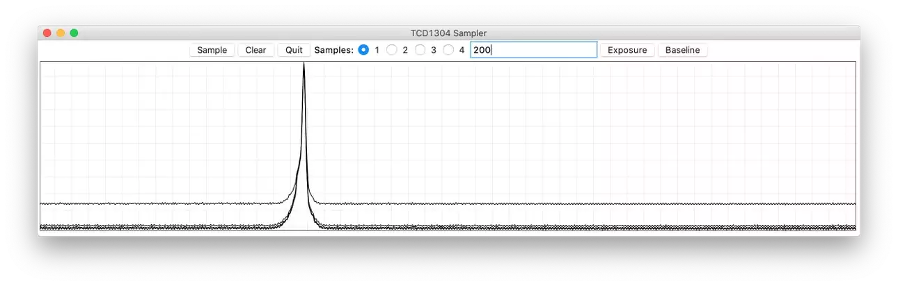
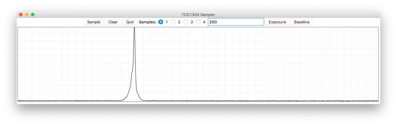
Adjust the exposure time until you get a maximum linear output from the spike. When the spike stops linearly increasing in height, stop increasing the exposure time. In the following image, you can see the curves getting linearly higher in amplitude, then going non-linear on the last step. I started at 100mS and worked up by 50mS per step to 250mS. 200mS was the last linear improvement, so I chose that as the working expoure time for the calibration procedure. The non-linearity is due to sensor saturation.
Clear and take a single sample at the current settings.
Adjust "Vref (+)" counter-clockwise, taking samples along the way, until the bottom line of the signal just reaches about to the bottom of the graph. It may take several turns of the pot to get there. If you overshoot, turn the pot the other direction to bring it back up.
Clear and take a single sample at the current settings.
Turn "Vref (-)" clockwise, taking samples along the way, until the tip of the peak just touches the top line. If you overshoot, you can bring it back down. It will bring the bottom up a bit, but we will tune that out later.
Clear and take a single sample at the current settings.
Go back to the "Vref (+)" pot and turn it counter-clockwise to bring the bottom back down.
Clear and take a single sample at the current settings.
Finally, if needed, back to the "Vref (-)" pot to pull the top up again. I didn't need it in this case, but only because I lucked out and hit it right the first time. If you want to get closer, keep repeating these last two steps until you are satisfied. The amplitude is not calibrated, but it is linear, if the last linear exposure time was chosen above. What this calibration does is increase the digital resolution to use as many of the 256 steps as possible.
You must adjust the pots in that order because, as you saw above, they interact with each other. That is by design. The maximum voltage you can put on Vref(-) is the voltage on Vref(+), and the minimum is ground, so changing Vref(+) changes the range and the current value of Vref(-).
When you remove the tape, clean the CCD glass with alcohol to get any residue off of it.
From now on, you use the exposure time to increase or decrease the range of the signal. If the line goes off the top of the graph, lower the exposure time, and if it falls short, increase the exposure time. If 1000mS isn't long enough, you can change it in the Python Sampler and in the Arduino IDE (both) to be whatever you need it to be. Noise increases with exposure time. If you need it to be shorter, we may need to experiment with microsecond timers. Send me some info on what you are doing via the Contact Form and I'll see what can be done.
Mechanics
Here is where we all go our separate ways. If you want a Raman spectrometer, you will be adding a laser, a grating, and a few mirrors. If you want a barcode reader, you will add a lens. My particular use for this was to characterize dichroic color separation filters used in CCD astrophotography. To do that, I needed a collimated light source, a stage for the filter, a slit, a transmission grating, and the board. I used a 1000 lines per mm Edmund Optics holographic grating in a 2" x 2" slide card.